Plasma-in-liquid PROTECTIVE COATING
Plasma-in-liquid coating

Large and non-uniform micro-arcs are the characteristics of the traditional coating process. However, the poorly-controlled large arcs cause:
(1) uneven coating
(2) burning at the edge
(3) excessive heating
Proprietary technology

Our proprietary technology allows only tiny plasma spreading across the sample surface uniformly, to
(1) promote uniform coating growth
(2) reduce damage to the parts
(3) minimize heating
Thus, our coating process is more controllable and energy-efficient.
In-house capability
We have world-class advisors and technical experts on the coating technology. We are committed to deliver excellent products for our clients.
Superior performance
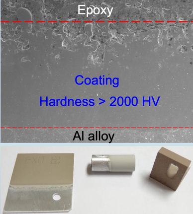
We are constantly pushing the limits of our coating, which represents the best-of-class with:
(1) High hardness (> 2000 HV)
(2) High dielectric breakdown voltage (> 2000 V)
(3) Excellent corrosion-resistance
(4) Conformal coverage along the contour of the 3D parts
Specially developed for semicon

The coating is specially developed to protect critical parts inside the plasma etching chamber for semiconductor manufacturing. With its high tolerance on dielectric breakdown and corrosion, it enables our ALE tools with high reliability and low maintenance costs.
Open for collaboration

Want to find out more on how our coating can transform your products, please feel free to contact us.